PCI/cPCI-VME link/interface (SIS1100/3100)
The SIS1100/SIS3100 PCI/cPCI to VME interface card combination was developed to meet the requirements of demanding VME data acquisition systems. The link is optimized for low latency high speed readout. Interaction with external logic is possible through optional input/output connectors on the VME side (SIS3100) of the link. The actual VME transactions are handled by a sequencer. The sequencer can execute VME cycles under PC program control or under control of the optional Digital Signal Processor (DSP).
The flexible FPGA based design allows for the implementation of the traditional VME cycles as well as more recent extensions to the standard, like 2eVME e.g.
Picture of SIS1100/3100 with DSP, SDRAM and front panel I/O option
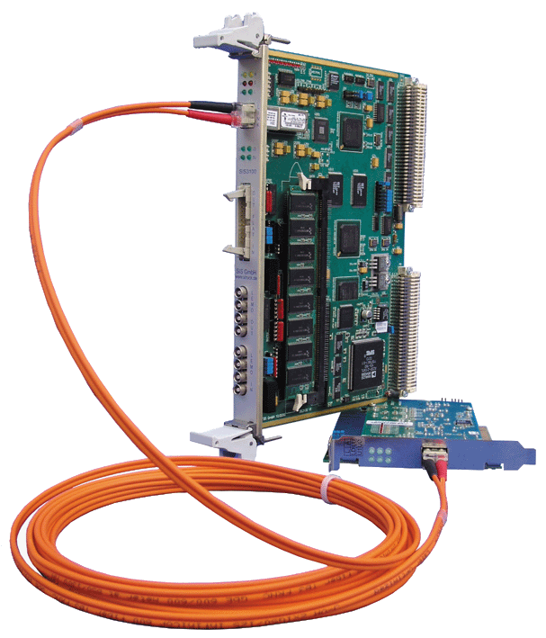
SIS1100/SIS3100 system setup

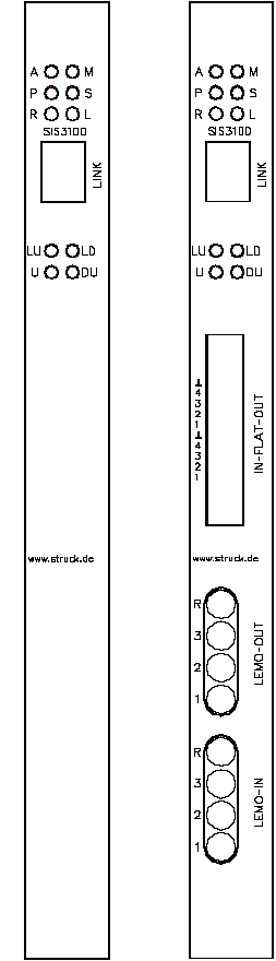
Properties of VME side:
(Base configuration)
|
LED's |
|
| A (access/slave) | M (master) |
| P (power) | S (sequencer) |
| R (ready) | L (link up) |
| LU (link data up) | LD (link data down) |
| U (user) | DU (dsp user) |
| Environment |
Performance |
|
| LINUX | BLT32 | 25 MBytes/s |
| MBLT64 | 50 MBytes/s | |
| 2eVME | >80 MBytes/s(*) | |
| Readout from SDRAM | 80 MBytes/s | |
| DSP VME single cycle | 600 ns/cycle | |
| measured with CI80 memory as VME slave | ||
| (*) measured with SIS3300 FADC as VME slave | ||
| Win2K/NI CVI | D32 | 5 µs/longword |
| mapped D32 read access | 3 µs/longword | |
| pipelined D32 write access | 700ns/longword | |
| MBLT64 read | 40 MBytes/s | |
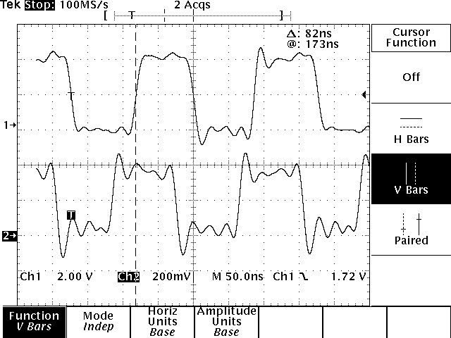
2eVME transfer scope shot
upper trace: DS1, lower trace: DTACK
Options
Front panel I/O option
Block diagram of VME side:

Properties of PCI/cPCI side:
The PCI (SIS1100) side consists of two printed circuit boards. The first board is a CMC carrier board (SIS1100-CMC or SIS1100-cCMC) with a PLX 9054 PCI master bridge chip a FPGA and glue logic, like boot circuitry, the second card is the CMC optical link mezaninne card (SIS1100-OPT).
Features of SIS1100-OPT
|
LED's on SIS1100-OPT |
|
| A (access) | L (link up) |
| LU (link data up) | LD (link data down) |
| U (user) | spare |
Software support:


Front panel design
Find below the front panel designs of the standard module (left hand side) and the design with front panel I/O option (right hand side)